
Albany opens shared EUV research access
Albany’s EUV Accelerator opened with standard-NA tools, while High-NA access was planned. Its shared research model connects chipmakers and technology partners.
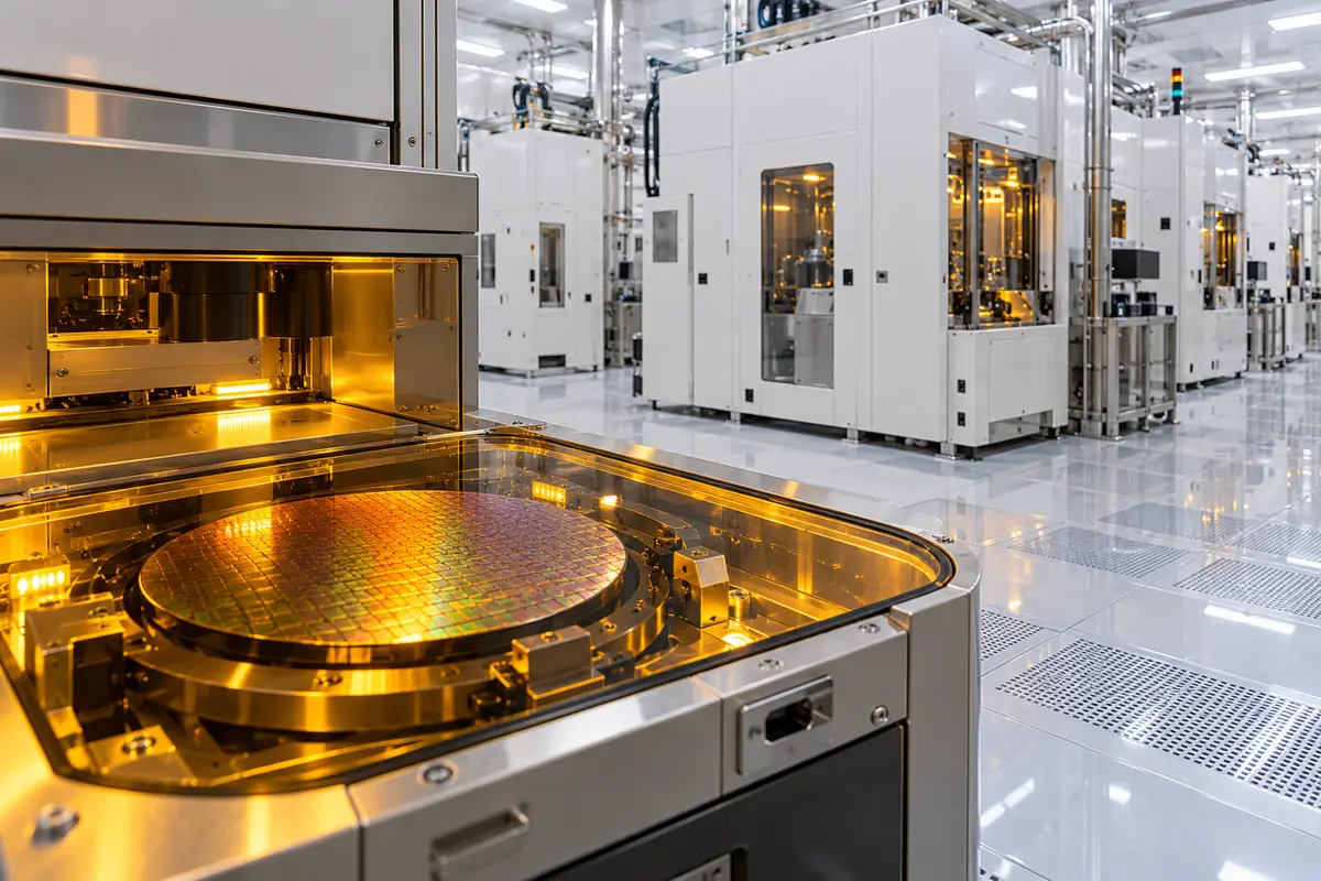
Shared research at Albany
The EUV Accelerator at NY Creates’ Albany NanoTech Complex began operations on July 1, 2025. Officials marked its opening on July 14 in New York, United States.
Natcast operates the facility for collaborative semiconductor research. Standard-numerical-aperture EUV access was available; High-NA access was expected in 2026.
Separate funding commitments
Governor Kathy Hochul’s announcement identified a $1 billion state investment covering an ASML EXE:5200 scanner and NanoFab Reflection, with more than 50,000 square feet of cleanroom space. A separate proposed federal investment totaled $825 million. The broader public-private partnership, announced in December 2023, was valued at $10 billion.

What changes with High-NA optics
ASML’s EXE platform uses the same 13.5-nanometer wavelength as its NXE EUV systems. Its numerical aperture increases from 0.33 to 0.55, improving the optical system’s ability to collect and focus light. ASML specifies an eight-nanometer resolution for the EXE:5000.
The larger mirrors required a different projection design. EXE’s anamorphic optics reduce the reticle pattern fourfold in one direction and eightfold in the other. This preserves compatibility with traditionally sized reticles while addressing the reflection problem created by a larger light-incidence angle.
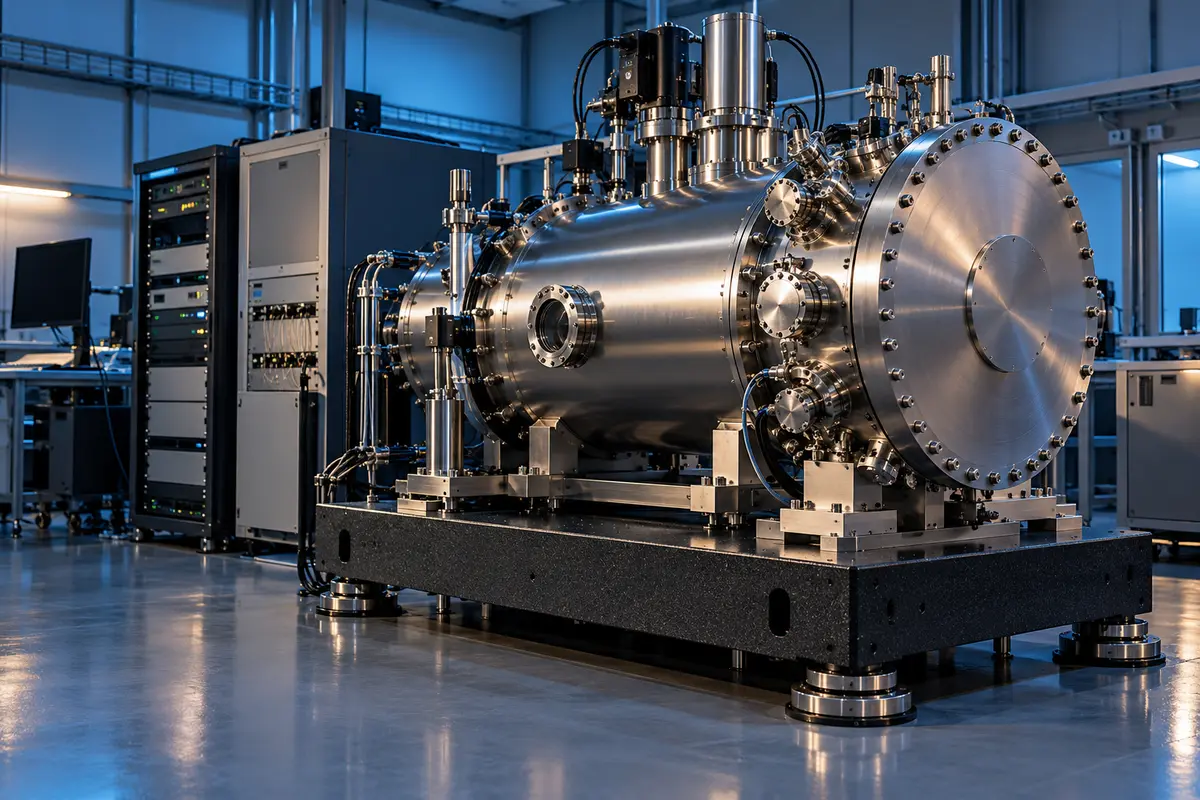
The exposure field is half the size of NXE’s, so a wafer requires more exposures. Faster wafer and reticle stages compensate for that smaller field. ASML’s design retains separate stages for positioning the wafer and the reticle during exposure.
The EXE system also reuses existing EUV technology. Its independently tested modules are integrated into the complete scanner, an approach intended to simplify installation at customer facilities. The first modules of the initial EXE:5000 shipped to Intel in December 2023.
Separate optical assemblies and measurement equipment
ZEISS, based in Germany, supplies the High-NA optical system. The projection optics contain more than 40,000 parts and weigh approximately 12 tonnes; the illumination system has roughly 25,000 parts and weighs more than six tonnes. The illumination system directs light, while the projection optics focus the pattern onto the wafer.
Mirror quality requires a separate metrology system. ZEISS developed that equipment with ASML and measures the mirrors in vacuum chambers about five meters in diameter. The measurement machine weighs 150 tonnes. These figures describe different assemblies and equipment, rather than the weight of one complete lithography scanner.

An earlier shared-access laboratory
ASML and imec opened a joint High-NA EUV Lithography Lab in Veldhoven, the Netherlands, on June 3, 2024. The European laboratory offered logic and memory chipmakers, materials suppliers and equipment companies access to an EXE:5000 prototype and surrounding tools. Its facilities included:
- A coating and development track;
- Metrology tools;
- Wafer and mask handling systems.
Early exposures printed 10-nanometer dense lines at a 20-nanometer pitch in metal-oxide resists. Those were prototype test results. Imec president Luc Van den hove described the laboratory as an extension of imec’s 300-millimeter cleanroom in Leuven, Belgium. ASML chief executive Christophe Fouquet said early access would let customers develop processes while awaiting their own systems. The partners anticipated high-volume manufacturing in 2025–2026.
Leave a comment