
Zeiss expands the factories behind semiconductor optics
Zeiss’s semiconductor expansion spans optics production, mask repair and customer qualification. The programme connects new buildings with ASML’s manufacturing plans.
A staged expansion in Oberkochen
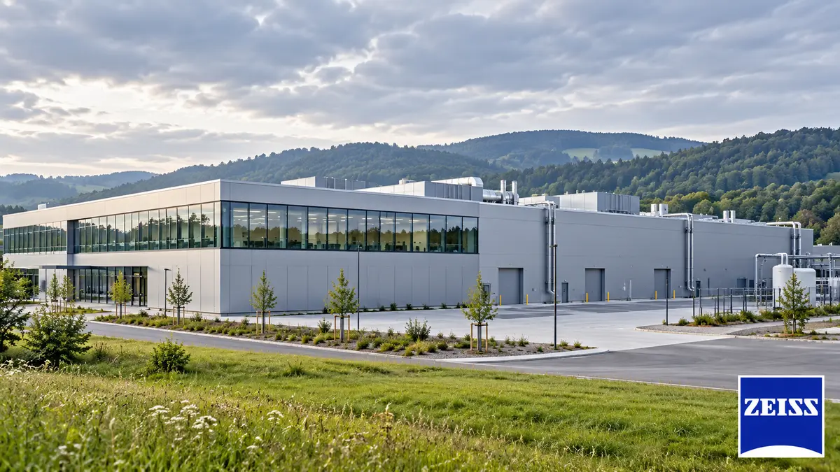
Zeiss Semiconductor Manufacturing Technology is adding around 25,000 square metres of production and production-related space in Oberkochen, Germany. Employees moved into the new office building in July 2026, around four years after the May 2022 groundbreaking. The remaining buildings are scheduled to enter operation in stages.
The programme extends across precision optics, photomask technologies and inspection. Frank Rohmund, president and chief executive of Zeiss SMT, connects the investment with the company’s long-term semiconductor strategy. The July office occupation is one completed milestone within the wider construction programme. A new company restaurant is also due to open.
Building beside sensitive production
The south factory in Oberkochen has expanded repeatedly since its 2001 groundbreaking. By September 2024, six major construction projects were running there in parallel, covering production areas, offices for production-related teams and a separate office building with a restaurant. Stefan-Albrecht Müller, head of central infrastructure at Zeiss SMT, identified this as the company’s largest capacity ramp-up. Construction takes place alongside existing operations, where measurement equipment is sensitive to disturbance from demolition and earthworks.

The buildings combine solid structures with demanding technical services. Cleanrooms require filter units and substantial ventilation equipment, while vibration requirements affect the underlying construction. Zeiss uses prefabricated elements, particularly for structural shells, together with coordinated transport and site logistics. The same September 2024 programme included the integration of Philips Engineering Solutions’ Aachen site, completed that February. Around 40 employees there worked on optical metrology equipment, following an earlier supplier relationship between the two businesses.
Wetzlar’s factory for DUV optics
Wetzlar’s new multifunctional factory broke ground on Mar 29, 2023, in the Dillfeld industrial zone. The project complements the existing downtown site, which was also being renovated. Its planned production area exceeds 12,000 square metres, with flexible spaces for optics, coating and assembly. Site manager Katrin Ariki explained that production-automation concepts tested in the existing factory would inform the new building. Sensitive measurement equipment required particular attention to a low-vibration building design.
The original plan envisaged around 150 skilled employees manufacturing products including DUV illumination systems. Wetzlar’s SMT workforce had grown from about 170 in 2017 to around 380 at the announcement. Zeiss then targeted more than 500 SMT jobs after completion in 2025. That was an earlier schedule: the July 2026 expansion announcement still described the multifunctional factory as under construction. More than 100 Consumer Products employees were separately manufacturing binoculars, spotting scopes and hunting optics at the existing location.

Dry and immersion lithography
DUV optics use several light wavelengths, including 365, 248 and 193 nanometres. Krypton-fluoride excimer lasers produce 248-nanometre light, while argon-fluoride systems operate at 193 nanometres. Dry lithography leaves air between the final lens and the wafer. Immersion lithography introduces a fluid into that gap. The fluid’s higher refractive index increases numerical aperture, improving the optical resolution available at the same wavelength. Zeiss has used immersion lithography since 2007.
Both dry and immersion systems remain in the company’s portfolio. Andreas Knipp, head of its DUV business, describes dry DUV as an established option for volume manufacturing, with operating and maintenance advantages. He also identifies demand for DUV optics alongside EUV and High-NA EUV. Different layers within a chip can require different exposure processes. DUV applications include smartphone touchscreen control, memory and automotive navigation. Wetzlar’s manufacturing expansion therefore serves an existing optical technology as well as the wider programme’s newer EUV capabilities.
More room for mask repair
Rossdorf’s development site opened an additional 300 square metres of cleanroom space on Sep 17, 2025. The completed expansion increased cleanroom area by 80% and provided room for four more specialised tools. It formed part of a wider investment package exceeding €20 million. Around 280 employees worked at the site, compared with about 80 in 2015. Zeiss acquired its predecessor, NaWoTec, a Deutsche Telekom spin-off, in 2005.
The Rossdorf team develops MeRiT mask-repair systems. Photomasks carry the patterns used to expose structures onto wafers; defects in those templates can affect production yield. The repair systems use electron beams to correct faults without physical contact. Development work takes place under clean, controlled and low-vibration conditions. The site maintains links with Darmstadt’s university and research community and cooperates with the Zeiss Innovation Hub at Karlsruhe Institute of Technology. The September 2025 opening figures supersede the earlier plan for a 50% cleanroom-area increase by the end of 2026.
Jena reaches the shell milestone
Jena’s new high-tech site celebrated its topping-out ceremony on May 13, 2025. Representatives from Zeiss, the city and the Free State of Thuringia attended. The building complex was then expected to provide around 118,000 square metres of floor space and to be completed by the end of 2026. Jena was Zeiss’s second-largest location worldwide, with around 3,500 employees at the time of the ceremony. The project extends the group’s founding location.
Andreas Pecher, president and chief executive of the Zeiss Group, presented the campus as part of its investment and modernisation strategy. Thuringia’s minister president, Mario Voigt, connected the investment with the region’s technological capabilities and employment. Dirk Lange, Jena’s head of urban development and environment, discussed the city’s role in supporting business growth. Guests viewed the shell through a drone tour before a crane raised the topping-out wreath, which project-team members and their children had prepared. The ceremony marked shell construction, ahead of the planned completion.

Customer qualification in Yongin
Zeiss opened its Semiconductor Innovation Center in Yongin on Jul 10, 2026. The centre brings together technologies from Semiconductor Mask Solutions and Semiconductor Fab Solutions for local development and customer qualification. Its programme covers high-volume wafer production, wafer-level packaging and photomask manufacturing. Rohmund and chief technology officer Thomas Stammler attended the opening, alongside the heads of the two business units, Karoline Piegdon and Clemens Neuenhahn. Jaane Seehusen also attended ahead of her scheduled appointment as head of Zeiss South Korea on Sep 1, 2026.
The equipment portfolio includes NLX-100 for three-dimensional X-ray metrology and inspection of package structures, and DUNE100 for measuring and correcting global wafer deformation. Zeiss also presented MeRiT AE as a future generation of mask-repair technology for particularly small and critical defects. Its prospective capabilities remain a development objective. Further equipment installations are planned. The centre gives Korean customers local access to evaluation and process work, with closer technical cooperation as its stated purpose.
The optical assembly and its measurements
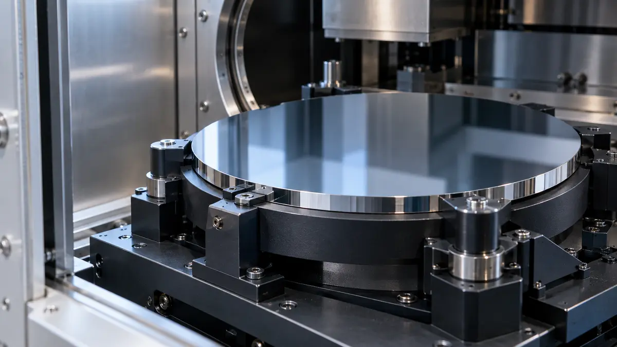
High-NA EUV optical systems combine large mechanical assemblies with highly precise mirrors. The projection optics contain more than 40,000 parts and weigh around twelve tonnes. The illumination system adds around 25,000 components and weighs more than six tonnes. Mirrors direct the exposure light through the scanner and focus it onto the wafer. More than 100 thin silicon and molybdenum layers are deposited onto their surfaces, each layer only a few atomic layers thick.

Peter Kürz, head of High-NA EUV at Zeiss SMT, explains that the larger numerical aperture allows more light to be captured and finer detail to be exposed. Zeiss and ASML developed specialised measurement equipment alongside the optics. The approximately 150-tonne measuring machine checks mirror quality in vacuum chambers around five metres in diameter. Zeiss’s January 2024 announcement, updated in January 2025, described roughly ten million research-and-development working hours devoted to High-NA EUV. These optical and measurement assemblies form part of the equipment requirements behind the manufacturing expansion.
Three decades of optical development
Zeiss’s EUV development programme includes several generations of optical hardware. A November 1995 workshop in Oberkochen brought together semiconductor manufacturers and research institutes around exposure at a wavelength of 13.5 nanometres. The 1999 micro-exposure tool provided projection optics for small illumination fields. Full-field EUV optics followed in 2006, with an EUV optics prototype in 2010. In 2012, Zeiss delivered its first standard EUV optics to ASML, followed by the launch of ASML’s TWINSCAN NXE:3300 in 2013.
The development path also included mask inspection: AIMS EUV arrived in 2017 to examine masks for defects under exposure conditions corresponding to those in wafer scanners. By May 2025, Zeiss had delivered more than 300 sets of EUV optics to ASML. Christoph Hensche, president of Semiconductor Manufacturing Optics, places those deliveries within a wider network of European partners. The systems combine precision mirrors and mechatronics, with development continuing toward High-NA EUV. The delivery total refers to optical sets at that date, rather than finished scanners manufactured during one year.
Operating and refurbishing the equipment
Zeiss SMT’s service teams assess components for repair, reuse and refurbishment. Tobias Berndt, the company’s sustainability team leader, says approximately 95% of the lithography systems it has delivered remain in use, many after 15–25 years. DUV accounts for a large majority of that installed population. Serviceability enters product development through component access, on-site repair and refurbishment of existing EUV components. Berndt also describes material and design changes to the Starlith 4200 illumination frame.
The company attributes an approximately two-thirds reduction in that frame’s carbon footprint to the redesign, compared with its previous generation. The claim concerns the frame, rather than the whole lithography system. Plant measures include closing unused exhaust ducts in two EUV production halls so that cleanroom air extraction matches requirements more closely. Standby vacuum pumps for High-NA measurement systems are activated when needed. In an Oberkochen hall, LED lighting replaced fluorescent tubes; a separate office-building solar installation contributes to the campus’s electricity supply.
Investment within a mixed group performance
Zeiss’s Semiconductor Manufacturing Technology segment generated revenue of €5.055 billion in fiscal 2024/25, compared with €4.122 billion a year earlier, an increase of 23%. The group’s financial year ended on Sep 30, 2025. Total group revenue reached €11.896 billion, up 9%, while earnings before interest and taxes amounted to €1.552 billion. Other businesses followed different paths: Industrial Quality & Research revenue declined slightly, while Medical Technology and Consumer Markets recorded increases.

The group invested €1.731 billion in research and development, equivalent to 15% of revenue, and €1.294 billion in property, plant and equipment. Those investment figures cover the entire group. Pecher identified continuing innovation as a priority despite geopolitical and market uncertainty. Chief financial officer Stefan Müller described cost awareness, process improvements and selective capacity adjustments across the businesses. At the year-end results announcement in December 2025, Zeiss expected another challenging financial year and said employment measures could include reduced overtime balances, short-time working and, in individual areas, job reductions.
Semiconductor growth and cost adjustments
For the first half of fiscal 2025/26, ending Mar 31, 2026, SMT revenue increased to €2.612 billion from €2.465 billion. Growth was 6% in reported terms and 7% after currency adjustment. Group revenue rose by 1% to €5.841 billion, with EBIT of €955 million. Industrial Quality & Research and Medical Technology recorded nominal declines, while Consumer Markets grew slightly. The group employed approximately 47,400 people worldwide at the reporting date.
In June 2026, Pecher identified two challenges: weak momentum in the direct-to-market businesses and structures accumulated during earlier rapid growth. Zeiss began preparing a competitiveness programme while retaining investment in innovation and markets. It targeted annual savings of several hundred million euros over three years against fiscal 2024/25, with measures to be developed through discussions with management and employee representatives. Job reductions were expected. The group’s first-half research spending was approximately €0.8 billion, or 14% of revenue; property, plant and equipment investment was around €0.4 billion.

ASML’s planned capacity increases
ASML’s July 2026 capacity plans cover both EUV and DUV immersion systems. Chief executive Christophe Fouquet linked the planned expansion to customer investment in advanced logic and memory. The programme separates a stated 2027 increase from a further expansion still under investigation:
- Low-NA EUV: add 30% in 2027 to 2026 capacity of around 65 systems.
- DUV immersion: add 30% in 2027 to 2026 capacity of around 130 systems.
- For both technologies, investigate another 30% capacity increase in 2028.
ASML also intends to expand its upgrade portfolio. These figures describe manufacturing capacity plans rather than completed system deliveries. The company’s second-quarter net sales were €9.326 billion, including €2.762 billion of installed-base management sales, which combine service and field options. It sold 86 new lithography systems and five used systems during the quarter. Fouquet attributed the stronger-than-guided result partly to installed-base activity. The July outlook retained uncertainty around demand, supply-chain capacity, product development and export controls.
The financing behind the optical columns
ASML holds 24.9% of Carl Zeiss SMT Holding, whose subsidiary supplies its optical columns. Development and testing use facilities in Oberkochen and Wetzlar. At Dec 31, 2025, ASML’s loans receivable from the Zeiss entities totalled €1.9075 billion, with €1.1919 billion of advance payments supporting future deliveries. Purchases reached €4.4069 billion in 2025, compared with €3.9465 billion in 2024 and €3.3259 billion in 2023. Separate loan agreements signed in 2021 and 2024 each originally allowed up to €1 billion. Further loans in July and November 2025 amounted to €444 million and €212.5 million respectively. Under the May 2025 framework restatement, qualifying capital-expenditure loans are interest-free, with expected terms of seven or fifteen years, a three-year grace period and revenue-linked quarterly repayments. Carl Zeiss AG provides a parental guarantee. The arrangements include work-in-progress advances settled through later optical-column deliveries, alongside High-NA research funding and contractual mechanisms supporting the supplier’s cash flow.
Leave a comment